
- GPR ™ Technology
- Alignment free
- Deflection compensation
- Roll and pitch axes


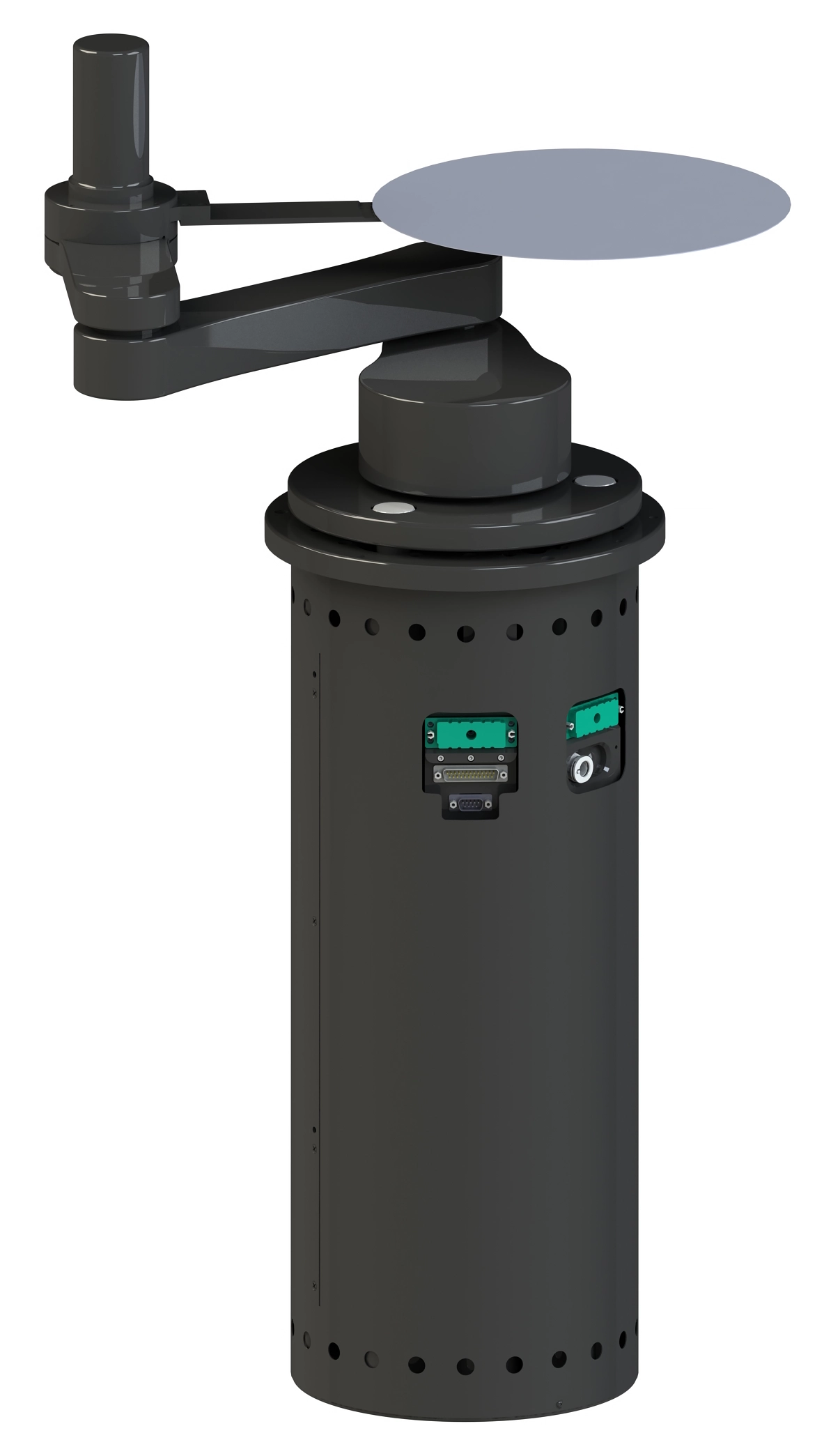
The GPR-GB7SY Yaw-Axis (single yaw) robot features Nidec Genmark’s technologically advanced mechanisms including patented GPR and YAW technologies to achieve the highest level of performance currently available in an automated material handler capable of transporting up to 300mm wafer payloads with utmost reliability and precision.
The patented GPR technology is based on a six-degree of freedom servo-controlled robot that can compliantly and intelligently interact with misaligned cassettes, FOUPS and process modules, as well as provide software-controlled end-effector deflection compensation during transport of heavier payloads.
The unique and patented YAW technology feature of the GPR-G7SY Robot system enables it to access in-line process modules, FOUPS and cassettes from a fixed centralized location, and eliminates the need for radial placement of process and other stations around the robot.
The GPR-GB7SY is capable of accessing up to four in-line FOUPS and dimensionally-equivalent process modules without the need to mount the robot on a linear track. The GPR-GB7SY can be fitted with numerous arm configurations and single or dual end-effectors thus allowing it to accommodate the automation requirements of a wide range of semiconductor manufacturing tool applications.
- Yaw axis
- Faster and more reliable robot movement
| Configuration | |
|---|---|
| Substrate Size | up to 300mm |
| Arm Configurations | 3 Link 6"-12"6" 3 Link 4"-8"-4" 2 Link 8"-8' |
| End Effector | Vacuum, Edge-Gripping, Gravity |
| Wafer Mapping | Reflective, through-beam, laser scanner, retro reflective (requires installation of reflective tape behind wafer carriers) |
| Physical Properties | |
| Size (body diameter) | 9.96" |
| Axes | 6: T, R, Y, Z, Z1, Z2 |
| Range of Motion | T: 500° R: - 6"-12"-6": [-22.8", 22.8"] - 4"-8"-4"; [-17.1", 17.1"] - 8"-8": [-22.8", 22.8"] Z: 17"; 20" Y: 344° Tilt: 1.5° |
| Performance | |
| Payload | 2.5 lbs |
| Repeatability | T: +/- 0.01° R: +/- 0.001" Z: +/- 0.001" Y: +/- 0.005° |
| Environment | |
| Cleanliness | ISO Class 1 Compatible |
| Wafer Contact Materials | Vespel, Peek, Teflon impregnated anodized AI, Alumina, Stainless Steel |
| Standards Compliance | |
| Applicable Directives/Standards | Machine Directive 89/392/EEC Low Voltage Directive 73/23/EEC 89/336/EEC(EMC) SEMI S2-93A |
| Standards to Verify Compliance | EN 60204-1:1997 EN 55011 EN ISO 12100-2:2003 RIA R15.06:1999 |
| Reliability per SEMI E10 | >15M MCBF |
